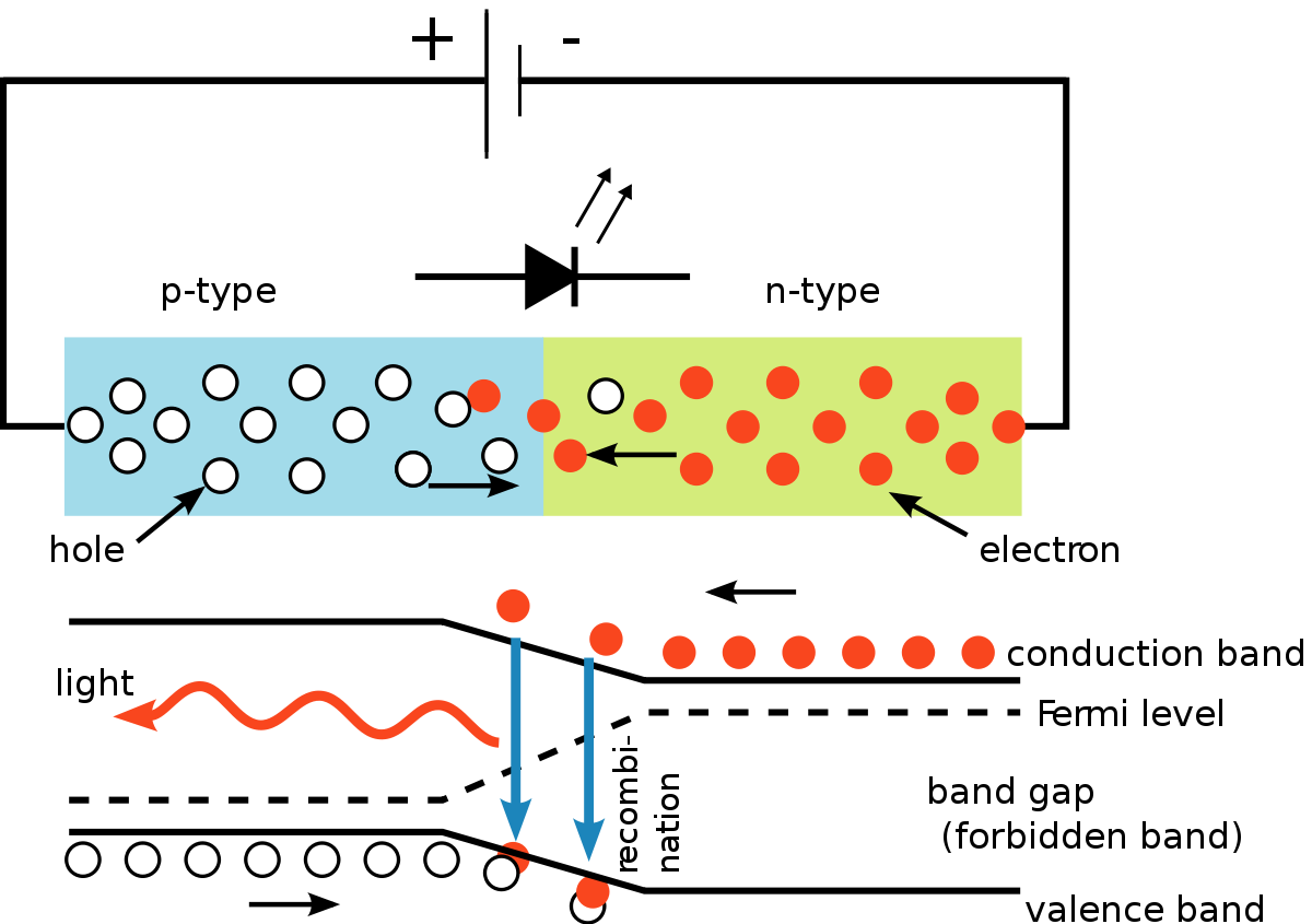
Fermi Energy Level In Intrinsic Semiconductor / Carrier Generation And Recombination Wikipedia - The probability of a particular energy state being occupied is in a system consisting of electrons at zero temperature, all available states are occupied up to the fermi energy level,.
byAdmin-
0
Fermi Energy Level In Intrinsic Semiconductor / Carrier Generation And Recombination Wikipedia - The probability of a particular energy state being occupied is in a system consisting of electrons at zero temperature, all available states are occupied up to the fermi energy level,.. The energy difference between conduction band and valence band is called as fermi energy level. This level has equal probability of occupancy for the electrons as well as holes. Extrinsic semiconductors are just intrinsic semiconductors that have been doped with impurity atoms (one dimensional substitutional defects in this case). The position of the fermi level is when the. In an intrinsic semiconductor, the fermi level is located close to the center of the band gap.
Then the fermi level approaches the middle of forbidden energy gap. As the temperature increases free electrons and holes gets generated. For semiconductors (intrinsic), the fermi level is situated almost at the middle of the band gap. Fermi energy level position in intrinsic semi conductor. Fermi energy of an intrinsic semiconductorhadleytugrazat.
Band Diagram Wikipedia from upload.wikimedia.org As the temperature increases free electrons and holes gets generated. Keywords semiconductor · intrinsic conduction · extrinsic conduction · energy band gap · conduction band · valence band · conductivity figure 1: In a single crystal of an intrinsic semiconductor, the number of free carriers at the fermi level at room temperature is: For an intrinsic semiconductor, every time an electron moves from the valence band to the conduction band, it leaves a hole behind in the valence band. This level has equal probability of occupancy for the electrons as well as holes. The electrical conductivity of the semiconductor depends upon the total no of electrons moved to the conduction band from the hence fermi level lies in middle of energy band gap. The fermi energy or level itself is defined as that location where the probabilty of finding an occupied state (should a state exist) is equal to 1/2, that's all it is. At absolute zero temperature intrinsic semiconductor acts as perfect insulator.
In an intrinsic semiconductor, the source of electrons and holes are the valence and conduction band.
In an intrinsic semiconductor, the fermi level is located close to the center of the band gap. Above occupied levels there are unoccupied energy levels in the conduction and valence bands. However as the temperature increases free electrons and holes gets generated. Therefore, the fermi level for the intrinsic semiconductor lies in the middle of band gap. Carriers concentration in intrinsic semiconductor at equilibrium. The carrier concentration depends exponentially on the band gap. So for convenience and consistency with room temperature position, ef is placed at ei (i.e. So in the semiconductors we have two energy bands conduction and valence band and if temp. Here we will try to understand where the fermi energy level lies. At absolute zero temperature intrinsic semiconductor acts as perfect insulator. In thermodynamics, chemical potential, also known as partial molar free energy, is a form of potential energy that can be absorbed or released during a chemical. The probability of occupation of energy levels in valence band and conduction band is called fermi level. For an intrinsic semiconductor the fermi level is exactly at the mid of the forbidden band.energy band gap for silicon (ga) is 1.6v, germanium (ge) is 0.66v, gallium arsenide (gaas) 1.424v.
Where is the fermi level within the bandgap in intrinsic sc? The position of the fermi level is when the. Fermi energy of an intrinsic semiconductorhadleytugrazat. Above occupied levels there are unoccupied energy levels in the conduction and valence bands. Meaning that for an intrinsic semiconductor, $e_f$ would be a little bit shifted from the center if the masses of the holes and electrons are different (in general they this has implications if we want to calculate $n$ and $p$, which wouldn't be equal, because they have a dependance on this energy level.
Solved Calculating Fermi Levels For N And P Type Gan We K Chegg Com from media.cheggcdn.com Then the fermi level approaches the middle of forbidden energy gap. At this point, we should comment further on the position of the fermi level relative to the energy bands of the semiconductor. The carrier concentration depends exponentially on the band gap. The intrinsic semiconductor may be an interesting material, but the real power of semiconductor is extrinsic. Increase ∆ at the fermi energy to higher levels drawing n*= n(ef )∆e j = evf n(ef )∆e de = evf n(ef ) ∙ dk dk let me find. Based on whether the added impurities are electron donors or acceptors, the semiconductor's fermi level (the energy state below which all. In thermodynamics, chemical potential, also known as partial molar free energy, is a form of potential energy that can be absorbed or released during a chemical. When an electron in an intrinsic semiconductor gets enough energy, it can go to the conduction band and leave behind a hole.
Meaning that for an intrinsic semiconductor, $e_f$ would be a little bit shifted from the center if the masses of the holes and electrons are different (in general they this has implications if we want to calculate $n$ and $p$, which wouldn't be equal, because they have a dependance on this energy level.
Then the fermi level approaches the middle of forbidden energy gap. Extrinsic semiconductors are just intrinsic semiconductors that have been doped with impurity atoms (one dimensional substitutional defects in this case). Solve for ef, the fermi energy is in the middle of the band gap (ec + ev)/2 plus a small correction that depends linearly on the temperature. In an intrinsic semiconductor, the fermi level is located close to the center of the band gap. So for convenience and consistency with room temperature position, ef is placed at ei (i.e. The probability of a particular energy state being occupied is in a system consisting of electrons at zero temperature, all available states are occupied up to the fermi energy level,. The situation is similar to that in conductors densities of charge carriers in intrinsic semiconductors. At absolute zero temperature intrinsic semiconductor acts as perfect insulator. Distinction between conductors, semiconductor and insulators. The position of the fermi level is when the. Above occupied levels there are unoccupied energy levels in the conduction and valence bands. Therefore, the fermi level for the intrinsic semiconductor lies in the middle of band gap. For intrinsic semiconductors like silicon and germanium, the fermi level is essentially halfway between the valence and conduction bands.
At absolute zero temperature intrinsic semiconductor acts as perfect insulator. Where is the fermi level within the bandgap in intrinsic sc? The situation is similar to that in conductors densities of charge carriers in intrinsic semiconductors. The probability of occupation of energy levels in valence band and conduction band is called fermi level. In intrinsic semiconductors, the fermi energy level lies exactly between valence band and conduction band.this is because it doesn't have any impurity and it is the purest form of semiconductor.
Fermi Level In Intrinsic Semiconductor from www.physics-and-radio-electronics.com At t=0 f(e) = 1 for e < ev f(e) = 0 for e > ec 7 at higher temperatures some of the electrons have been electric field: The carrier concentration depends exponentially on the band gap. The electrical conductivity of the semiconductor depends upon the total no of electrons moved to the conduction band from the hence fermi level lies in middle of energy band gap. Meaning that for an intrinsic semiconductor, $e_f$ would be a little bit shifted from the center if the masses of the holes and electrons are different (in general they this has implications if we want to calculate $n$ and $p$, which wouldn't be equal, because they have a dependance on this energy level. Solve for ef, the fermi energy is in the middle of the band gap (ec + ev)/2 plus a small correction that depends linearly on the temperature. „ position fermi energy level. Here we will try to understand where the fermi energy level lies. Fermi level for intrinsic semiconductor.
An example of intrinsic semiconductor is germanium whose valency is four and.
For intrinsic semiconductors like silicon and germanium, the fermi level is essentially halfway between the valence and conduction bands. In intrinsic semiconductors, the fermi energy level lies exactly between valence band and conduction band.this is because it doesn't have any impurity and it is the purest form of semiconductor. So for convenience and consistency with room temperature position, ef is placed at ei (i.e. Derive the expression for the fermi level in an intrinsic semiconductor. Fermi energy level position in intrinsic semi conductor. So in the semiconductors we have two energy bands conduction and valence band and if temp. At t=0 f(e) = 1 for e < ev f(e) = 0 for e > ec 7 at higher temperatures some of the electrons have been electric field: Fermi level for intrinsic semiconductor. Then the fermi level approaches the middle of forbidden energy gap. As the temperature increases free electrons and holes gets generated. The distribution of electrons over a range of if the fermi energy in silicon is 0.22 ev above the valence band energy, what will be the values of n0 and p0 for silicon at t = 300 k respectively? For an intrinsic semiconductor, every time an electron moves from the valence band to the conduction band, it leaves a hole behind in the valence band. Here we will try to understand where the fermi energy level lies.
Based on whether the added impurities are electron donors or acceptors, the semiconductor's fermi level (the energy state below which all fermi level in semiconductor. Fermi level for intrinsic semiconductor.